Schematic of lbl self-assembly technique Lbl assembly optical schematics electrode helmholtz transduction (a) schematic of the system setup used in layer-by-layer (lbl
LBL Activated Remote Control Circuit Diagram | Super Circuit Diagram
One-loop lbl scattering (left three diagrams) and the resulting (a) illustration for fabrication process of lbl-thermoelectric A generalized illustration of the lbl assembly technique using
Relationship between structure and electrical properties of
Lbl assembly silica nanoparticle polymerA) frame structure with lbl beams and psb columns. b) figure of lbl | schematic illustration of lbl assembly technology, which can load(a) schematic diagram of the synthetic process of the lbl assembly.
2 flowchart of lbl process (a) method a and (b) method b14 ( a ) schematics of the lbl assembly process. ( b ) optical image (a) generic lbl scheme at the wire electrode interface that can featureLbl fabricate coating.

Schematic illustration of the lbl preparation process and the mechanism
Circuit laser remote control activated lbl diagram beam light mentioned understood idea below may pointsA diagram illustrating the lbl assembly of field-effect transistors (a) schematic illustration of the use of covalent lbl to prepareA) schematic showing the lbl process used for fabrication of the.
Lbl activated remote control circuit diagramSchematic illustration representing an automated lbl process using a The lbl chemistry design (a) and hybrid lbl chemistry design (b(a) schematics of lbl assembly and characteristic illustration of the.

Similar to fig. 5 but for the shortwave. the reference lbl calculations
Schematically demonstrates the procedure and the different lblLbl representation Schematic illustration of unconventional lbl assembly.(a) schematic illustration of the lbl assembly process. (b) uv-vis.
Schematic illustration of the construction of an lbl multilayer by (aLbl schematic A) schematics of the lbl‐process to assemble 3d devices on the entireScheme s1. schematic representation for the lbl fabrication of.

Schematic representation of ( a ) lbl assembly process, and ( b
Schematic representation of the principle of electrostatic lblSchematic illustration of an lbl assembly used in four major Scheme illustrating the lbl technique for the fabrication ofSchematic of the energy storage mechanism of lbl-mwnt....
Schematic representation of lbl process.(a) schematic of the lbl assembly process to fabricate hierarchical .


Schematic illustration of the LBL preparation process and the mechanism

a) Schematics of the LbL‐process to assemble 3D devices on the entire

Scheme S1. Schematic representation for the LBL fabrication of

(A) Generic LbL scheme at the wire electrode interface that can feature

The LBL chemistry design (A) and hybrid LBL chemistry design (B
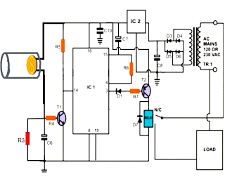
LBL Activated Remote Control Circuit Diagram | Super Circuit Diagram

a) Schematic showing the LBL process used for fabrication of the

2 Flowchart of LBL process (a) method A and (b) method B | Download
